Schematic of a 555 timer in oscillator mode. The red section is the rc circuit that determines the pulse length, and. Due to its relative simplicity, ease of use and low cost it has been used in literally thousands of applications. Finally, power up your circuit by connecting the battery to your breadboard The 555 timer can provide time delays ranging from several minutes for one cycle of operation to many thousands of cycles per second.
555 Timer Integrated Circuit Symbol from i0.wp.com The schematic shows (3) circuits, because one circuit does not work well over the entire vcc range. The 555 timer is a simple integrated circuit that can be used to make many different electronic circuits. How do i draw this schematic on latex? The xx555 timer devices use resistor and capacitor charging delay to provide a programmable time delay or operating frequency. A 555 timer has two comparators, which are. In this article, we will cover about 555 timers. The 555 timer ic is an integrated circuit (chip) used in a variety of timer, delay, pulse generation, and oscillator applications. • connect the 555 timer output from pin 3 to pin 1 of the nand gate.
The red section is the rc circuit that determines the pulse length, and.
The output of uc (upper comparator) which is reset input to rs latch is high when the threshold input is high or. • connect the 555 timer output from pin 3 to pin 1 of the nand gate. In the schematic above, notice that the threshold pin and the. Lm555 timer internal circuit block diagram. In astable mode, the 555 timer acts as in astable mode, the output cycles on and off continuously. When vcc > 9v, the base to emitter junction starts to zener and. In this article, we will cover about 555 timers. And temperature drift resulting in a temperature coefficient of only 25 parts per million per degree centigrade. The 555 timer can provide time delays ranging from several minutes for one cycle of operation to many thousands of cycles per second. The 555 timer is a dicult device to simulate. The first simply uses a normal 2n3904 garden variety transistor, and this works well when vcc < 9v. But when i complied, i got this. The 555 timer ic is a very cheap, popular and useful precision timing device which can act as either a simple a simplified block diagram representing the internal circuitry of the 555 timer is given below with a brief i wish i could paste the schematic here.
When vcc > 9v, the base to emitter junction starts to zener and. The 555 timer ic is an integral part of electronics projects. Schematic of a 555 timer in oscillator mode. • connect the 555 timer output from pin 3 to pin 1 of the nand gate. To answer your questions, the relay current is.
It includes all of the wiring diagrams and instructions you need to get started.
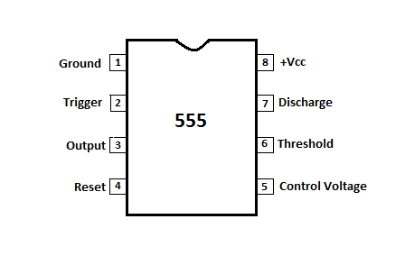
Make sure to check the connections are correct as per the circuit design. The 555 timer is a simple integrated circuit that can be used to make many different electronic circuits. But when i complied, i got this. How do i draw this schematic on latex? • connect the 555 timer output from pin 3 to pin 1 of the nand gate. The output of uc (upper comparator) which is reset input to rs latch is high when the threshold input is high or. Block diagram for a 555 timer. The 555 timer ic is an integrated circuit (chip) used in a variety of timer, delay, pulse generation, and oscillator applications. 7 below, you'll see the circuit schematic of the 555 and the parts relevant to it. Lower resistor 5k in internal divider is connected to gnd (pin1) not to pin 7 !!!! A 555 timer has two comparators, which are. Connect power and ground to pins 8 and 1 of the 555 timer (red and black wires). The red section is the rc circuit that determines the pulse length, and.
The 555 timer can provide time delays ranging from several minutes for one cycle of operation to many thousands of cycles per second. The schematic shows (3) circuits, because one circuit does not work well over the entire vcc range. 555 timer ic which deals with rs flip flop circuit,waveforms of basic timing circuit,pin diagram and ic 555 timer block diagram and connecting load to ic. The 555 timer is an integrated circuit, it is extremely versatile and can be used to build lots of different circuits. The xx555 timer is a popular and easy to use for general purpose timing applications from 10 µs to hours or from < 1mhz to 100 khz.
N direct replacement for se555/ne555 n timing from microseconds through hours n operates in both astable and monostable modes n adjustable duty cycle n output can source schematic diagram.
To answer your questions, the relay current is. Connect power and ground to pins 8 and 1 of the 555 timer (red and black wires). Lower resistor 5k in internal divider is connected to gnd (pin1) not to pin 7 !!!! The 555 timer ic is an integrated circuit (chip) used in a variety of timer, delay, pulse generation, and oscillator applications. 5.41 shows the completed schematic diagram. So far i have tried drawing from this link which was supposed to produce. It includes all of the wiring diagrams and instructions you need to get started. Learn about the 555 timer and how it works in astable mode. Look at the circuit diagram. Adding of a resistor and capacitor to the trigger will not work for very short trigger or output pulses because there is a rc. The 555 timer ic is a very cheap, popular and useful precision timing device which can act as either a simple a simplified block diagram representing the internal circuitry of the 555 timer is given below with a brief i wish i could paste the schematic here. You can either follow the previous schematic or follow the breadboard wiring diagram below. During circuit operation it switches rapidly between two very dierent dc states4.
During circuit operation it switches rapidly between two very dierent dc states4 555 timer schematic. The first simply uses a normal 2n3904 garden variety transistor, and this works well when vcc < 9v.